
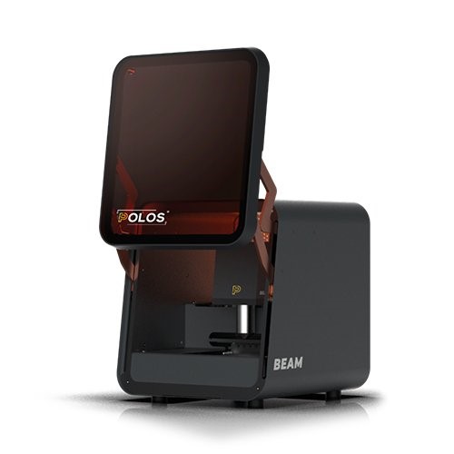
The SPS POLOS BEAM Series (Lite Mk2, Mk2, and XL Mk2) are advanced mask less lithography systems designed for precision microfabrication, semiconductor prototyping, MEMS development, photonics research, and nanotechnology applications. Engineered for R&D laboratories, universities, cleanrooms, and pilot production environments, the systems deliver high-resolution direct laser writing in compact and scalable configurations.
By eliminating conventional photomasks, the BEAM Series reduces lithography cycle times, lowers operational costs, and accelerates process development. CAD-based pattern data is directly transferred onto photoresist-coated substrates using precision UV laser exposure, enabling rapid prototyping, multilayer processing, and flexible design iteration.
With advanced optics, precision motion control, and automated focusing technology, the systems provide reliable high-resolution lithography with excellent repeatability, overlay accuracy, and process stability.
The SPS POLOS BEAM Series supports a broad range of microfabrication applications, including:
Specification | POLOS BEAM Lite Mk2 | POLOS BEAM Mk2 | POLOS BEAM XL Mk2 |
Resolution | 1.5 µm / 3 µm | 0.8 µm | 0.8 µm |
Lithography Method | UV Direct Laser Writing | UV Direct Laser Writing | UV Direct Laser Writing |
Max Substrate Size | 4″ (100 × 100 mm) | 4″ (100 × 100 mm) | 6″ (150 × 150 mm) |
Max Exposure Area | 106 × 106 mm | 106 × 106 mm | 155 × 155 mm |
Writing Modes | Vector / Raster | Vector / Raster | Vector / Raster |
Light Source | Laser Galvo / Laser Diode | Laser Galvo / Laser Diode | Laser Galvo / Laser Diode |
Standard Wavelength | 405 nm | 405 nm | 405 nm |
Optional Wavelength | 375 nm | 375 nm | 375 nm |
Alignment Resolution | 0.1 µm | 0.1 µm | 0.1 µm |
Stage Repeatability | 0.1 µm | 0.1 µm | 0.1 µm |
Maximum Writefield | 400 µm | 400 µm | 400 µm |
Writing Speed | ≥ 2 mm/s | ≥ 2 mm/s | ≥ 2 mm/s |
Autofocus Range | ±100 µm | ±100 µm | ±100 µm |
Grayscale Option | 256 Levels | 256 Levels | 256 Levels |
Alignment Type | Topside | Topside / BSA (Optional) | Topside / BSA (Optional) |
Compatible File Formats | BMP, PNG, TIFF, GDS | BMP, PNG, TIFF, GDS | BMP, PNG, TIFF, GDS |
Photoresist Compatibility | h-line, Broadband, SU8 | h-line, Broadband, SU8 | h-line, Broadband, SU8 |
Max Resist Thickness | 10 µm | 10 µm | 10 µm |
Software | BEAM Xplorer | BEAM Xplorer | BEAM Xplorer |
Utility Requirement | Only Electricity | Only Electricity | Only Electricity |
The SPS POLOS BEAM Series combines high-resolution direct laser writing, precision alignment, advanced motion control, and compact system integration into a powerful mask less lithography platform for modern microfabrication environments.
Designed for semiconductor research, MEMS fabrication, photonics, and nanotechnology development, the systems enable high-performance lithography with reduced process complexity and accelerated innovation cycles.
Request technical specifications
Discuss process compatibility
Schedule a live demonstration
Explore system configurations and integration options


ISO 9001:2015 Certified Quality Management System
Certified by Intertek – UKAS Accredited
© 2026 HTL Co India Pvt. Ltd. All Rights Reserved.