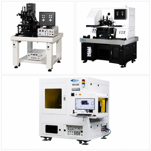
We offer a comprehensive range of 4″ to 12″ mask aligner systems designed for photolithography, wafer alignment, UV exposure, and microfabrication applications. Our portfolio includes manual, semi-automatic, and fully automatic mask aligners with UV-LED, NUV, and broadband UV lamp technologies to support both research and production environments.
These systems are widely used in semiconductor manufacturing, MEMS fabrication, advanced packaging, biochips, photonics, nanotechnology, and university research laboratories, delivering high alignment accuracy, excellent exposure uniformity, and reliable process repeatability.
Choose from manual, semi-automatic, and fully automatic platforms to match your throughput, process control, and production requirements.
Alignment accuracy up to 0.5 µm enables reliable multilayer lithography, wafer bonding preparation, and advanced micro-patterning applications.
Available with:
Support for:
Allowing optimization for various photoresists, substrates, and lithography requirements.
From academic laboratories and R&D centres to pilot production and high-volume manufacturing, our mask aligners provide scalable lithography solutions for evolving process requirements.
Supports wafer-level photolithography, alignment, pattern transfer, and advanced packaging processes requiring high overlay accuracy and repeatability.
Ideal for sensors, actuators, microstructures, and other MEMS devices requiring precise multilayer alignment.
Enables fabrication of optical waveguides, photonic structures, micro-optics, and integrated optical components.
Supports fabrication of lab-on-chip devices, biosensors, microfluidic channels, and biomedical research platforms.
Widely used in nanofabrication facilities, cleanrooms, universities, and R&D centers for process development and prototyping.
Model | System Type | Mask Size | Substrate Size | UV Source | Wavelength | Alignment Accuracy |
MA-400X-A | Manual Touch Screen | Up to 4″ × 4″ | Up to 4″ | UV-LED | 365 nm | 1 µm |
MA-600X-A | Manual Touch Screen | Up to 6″ × 6″ | Up to 6″ | UV-LED | 365 nm | 1 µm |
MA-800X-A | Manual Touch Screen | Up to 8″ × 8″ | Up to 8″ | UV-LED | 365 nm | 1 µm |
MDA-400LJ | Manual | Up to 5″ × 5″ | Up to 4″ | UV-LED | 365 nm | 1 µm |
MDA-400M-6 | PC/PLC Controlled Manual | Up to 7″ × 7″ | Up to 6″ | 350 W UV Lamp | 350–450 nm | 1 µm |
MDA-80MS | Semi-Automatic | Up to 9″ × 9″ | Up to 8″ × 8″ | 1 kW UV Lamp | 350–450 nm | 1 µm |
MDA-12SA | Semi-Automatic | Up to 14″ × 14″ | Up to 8″ × 8″ | 2/5 kW UV Lamp | 350–450 nm | 1 µm |
MDA-60FA | Fully Automatic | Up to 7″ × 7″ | 4″–6″ Wafers | 350/500 W UV Lamp | 350–450 nm | 0.5 µm |
MDA-12FA | Fully Automatic | Up to 14″ × 14″ | 8″–12″ Wafers | 2/5 kW UV Lamp | 350–450 nm | 0.5 µm |
The SPS POLOS BEAM Series combines high-resolution direct laser writing, precision alignment, advanced motion control, and compact system integration into a powerful mask less lithography platform for modern microfabrication environments.
Designed for semiconductor research, MEMS fabrication, photonics, and nanotechnology development, the systems enable high-performance lithography with reduced process complexity and accelerated innovation cycles.
Our lithography specialists can help you select the right mask aligner based on wafer size, alignment accuracy, throughput, and process requirements.


ISO 9001:2015 Certified Quality Management System
Certified by Intertek – UKAS Accredited
© 2026 HTL Co India Pvt. Ltd. All Rights Reserved.