
for wafer scribing, substrate cutting, sample preparation, and device singulation. Available in 4″, 8″, and 12″ configurations, these laboratory-scale systems deliver excellent edge quality, high repeatability, and minimal substrate damage across a wide range of materials.
Designed for semiconductor laboratories, MEMS fabrication, photonics, nanotechnology, and materials research, POLOS wafer scribers combine ergonomic operation, adjustable pressure control, and precision-guided cutting for reliable wafer separation and prototyping workflows.
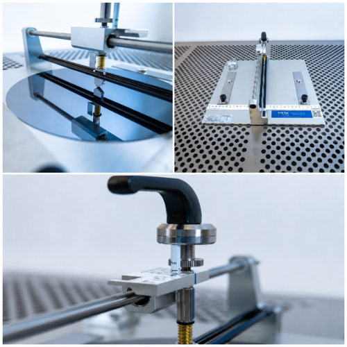
Precision-guided cutting enables repeatable wafer separation with cutting accuracy better than 0.1 mm and fine adjustment accuracy up to ±50 µm.
Integrated spring-loaded pressure adjustment ensures consistent scribing force, reducing cracking, chipping, and substrate damage.
Optimized wheel materials support a broad range of wafer types:
Compatible with:
Stable substrate positioning improves cut accuracy, dimensional consistency, and process repeatability.
Lightweight bench-top construction enables easy integration into cleanrooms, research laboratories, and prototyping facilities.
Available accessories include:
Accurate wafer scribing and substrate separation with excellent edge quality and minimal damage.
Ideal for sample preparation, prototype fabrication, and micro-device development.
Supports precision cutting of optical substrates and specialty materials.
Compact and user-friendly design makes it suitable for R&D laboratories, cleanrooms, and academic research facilities.
An efficient solution for low-volume production, process development, and laboratory wafer preparation.
Specification | 4″ Wafer Scriber | 8″ Wafer Scriber | 12″ Wafer Scriber |
Cutting Wheel | Diamond or Carbide | Diamond or Carbide | Diamond or Carbide |
Suitable Thickness | 0.05 – 3.0 mm | 0.05 – 3.0 mm | 0.05 – 3.0 mm |
Spring Pressure | 0 – 50 N | 0 – 50 N | 0 – 50 N |
Cutter Height Range | 0 – 5 mm | 0 – 5 mm | 0 – 5 mm |
Maximum Cut Length | 110 mm | 210 mm | 310 mm |
Wheel Length | 26 ± 0.05 mm | 26 ± 0.05 mm | 26 ± 0.05 mm |
Base Plate | Anodized Super-Flat Aluminum Alloy | Anodized Super-Flat Aluminum Alloy | Anodized Super-Flat Aluminum Alloy |
Dimensions (W × D × H) | 210 × 210 × 136 mm | 310 × 310 × 136 mm | 410 × 410 × 136 mm |
Weight | 1.37 kg | 2.41 kg | 4.25 kg |
SPS POLOS Wafer Scribers provide accurate and repeatable wafer cutting for semiconductor, MEMS, photonics, and materials research applications. With flexible substrate compatibility, adjustable cutting control, and multiple wafer size options, they offer an efficient solution for laboratory-scale wafer processing and device preparation


ISO 9001:2015 Certified Quality Management System
Certified by Intertek – UKAS Accredited
© 2026 HTL Co India Pvt. Ltd. All Rights Reserved.