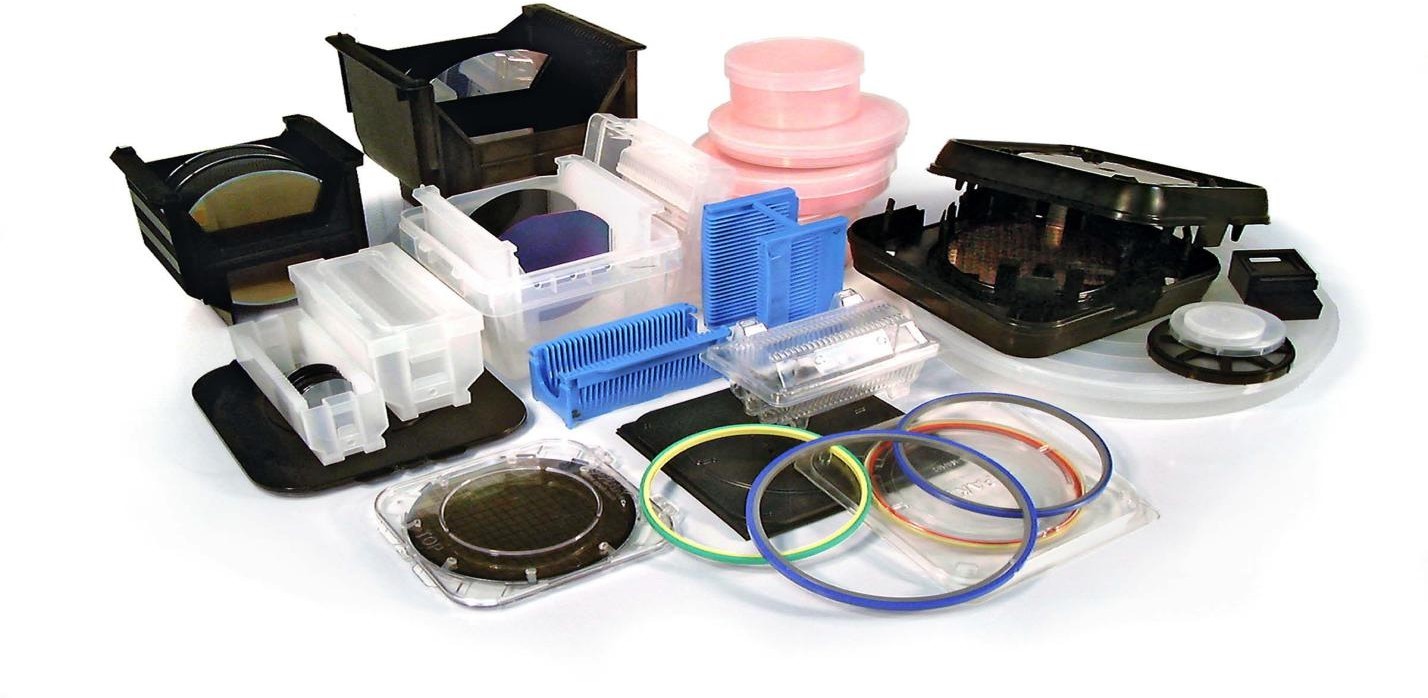
SPS POLOS offers a comprehensive range of wafer and photomask handling, storage, and transportation solutions designed for contamination-free semiconductor processing and cleanroom operation. The portfolio includes wafer shippers, storage boxes, canisters, cassettes, vacuum handling tools, and photomask handling accessories for safe substrate management throughout manufacturing and research workflows.
Engineered for semiconductor fabs, MEMS fabrication, photonics, advanced packaging, and research laboratories, these products help minimize particle contamination, handling damage, and wafer breakage while ensuring reliable cleanroom compatibility
Solutions for secure wafer storage, shipping, and cleanroom transfer:
Designed for safe wafer organization, transport, and process tool compatibility:
Precision handling solutions for contamination-free substrate transfer:
Designed to reduce particle generation and protect sensitive wafer surfaces during transport, storage, and processing.
Helps prevent scratches, chipping, breakage, and handling damage during manufacturing and logistics operations.
Manufactured using materials suitable for semiconductor and microfabrication environments.
Supports a wide range of wafer sizes, photomasks, substrates, and semiconductor materials.
Compatible with laboratory, pilot production, and semiconductor manufacturing workflows.
Safe wafer handling, storage, transport, and process tool loading across fabrication workflows.
Protection and transfer of delicate substrates used in MEMS, sensors, and advanced packaging applications.
Secure movement and storage of masks used in lithography and microfabrication processes.
Ideal for universities, nanofabrication centres, R&D facilities, and pilot production environments.
Product Number | Supported Size | Type | Configuration | ISO Class |
WHS-V2-SET-SD | Small Devices & Dies | Set | Precision Handling | ISO 4 |
WHS-V2-SET100C | 76–100 mm Wafers | Kit | Straight Grip | ISO 3 |
WHS-V2-SET200 | 150–200 mm Wafers | Set | Straight Bend | ISO 3 |
WHS-V2-SET200C | 150–200 mm Thin/Compound Wafers | Set | Straight Bend | ISO 3 |
WHS-V2-SET300 | 300 mm Wafers | Set | Straight Bend | ISO 3 |


ISO 9001:2015 Certified Quality Management System
Certified by Intertek – UKAS Accredited
© 2026 HTL Co India Pvt. Ltd. All Rights Reserved.