HTL Japan Founded
HTL Japan was founded by President Acharya to provide high-technology trading and liaison services in the semiconductor industry.
Delivering High-Technology Solutions for the Semiconductor Industry since 2012.
At HTL India, we take immense pride in contributing to India’s rapidly growing semiconductor and high-technology ecosystem—particularly through our strong alignment with the Make-in-India initiative. As a key player in semiconductor equipment sales and solutions, we are committed to
strengthening India’s position in global manufacturing by enabling advanced production capabilities locally.
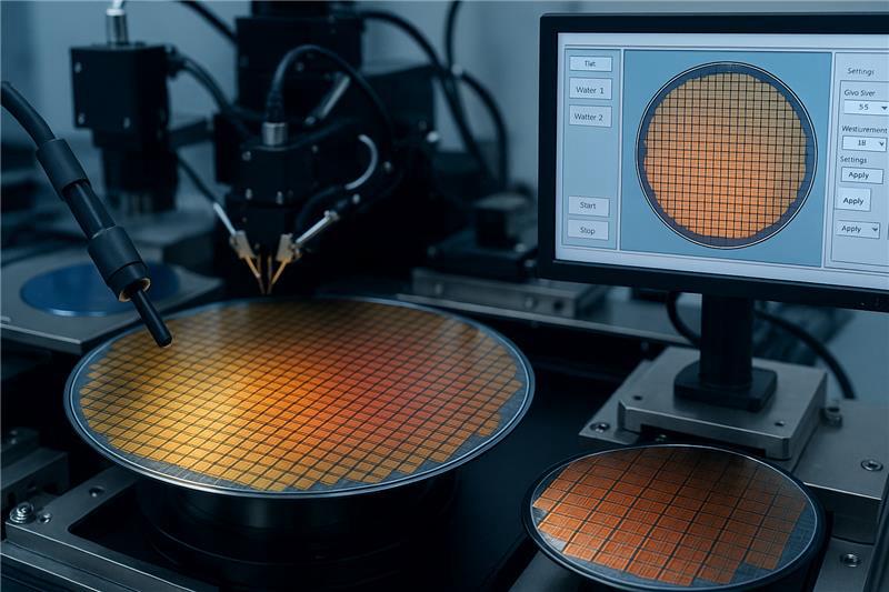
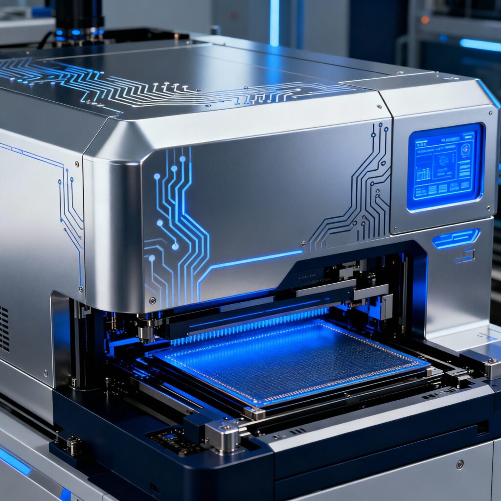
With our own cleanroom facility in Bangalore, HTL India delivers end-to-end hardware solutions for the semiconductor and electronics industries. Our portfolio spans lithography systems, wafer and panel fabrication equipment, Photomask & Flat panel display Mask writer, inspection, repair, CD systems, deposition tools, ESD solutions, ALD & MLD tools, Annealing equipment, metal 3D printers for additive manufacturing platforms, and associated FPD-related equipment—supported by comprehensive after-sales service and lifecycle support.
We are also deeply engaged in Outsourced Semiconductor Assembly and Test (OSAT) initiatives, photomask production support, wafer inspection, and nextgeneration automation. As part of our long-term roadmap, we are expanding our contribution to include raw material support for both front-end and backend semiconductor manufacturing, reinforcing India’s self-reliance in critical technologies.
In addition to our technology leadership, HTL India is strongly committed to talent development in the semiconductor ecosystem. We offer structured industrial semiconductor training programs along with internship opportunities for college graduates, enabling young engineers to gain handson exposure to real manufacturing environments and preparing them to contribute effectively to India’s growing high-technology industry.
As a wholly owned subsidiary of HTL Japan, established in 2012, HTL India is part of a group that has delivered advanced technology solutions to customers across Japan, the USA, Europe, South Korea, China, Taiwan, and India for more than three decades. Our unique strength in India lies in combining deep hardware expertise with strong local execution, supported by robust service, logistics, and engineering teams. We are also actively expanding our engagement with prestigious institutions such as IITs and national research organizations—supporting semiconductor laboratories, mini-fabs, and full-scale production environments to nurture the next generation of innovation.
Looking ahead, our vision is clear: HTL will not only supply world-class equipment, but deliver end-to-end integrated solutions—from advanced inspection and repair systems to system integration, process optimization, and full lifecycle services. Through this holistic approach, we aim to be a long-term strategic partner to our customers, enabling sustainable growth and operational excellence.
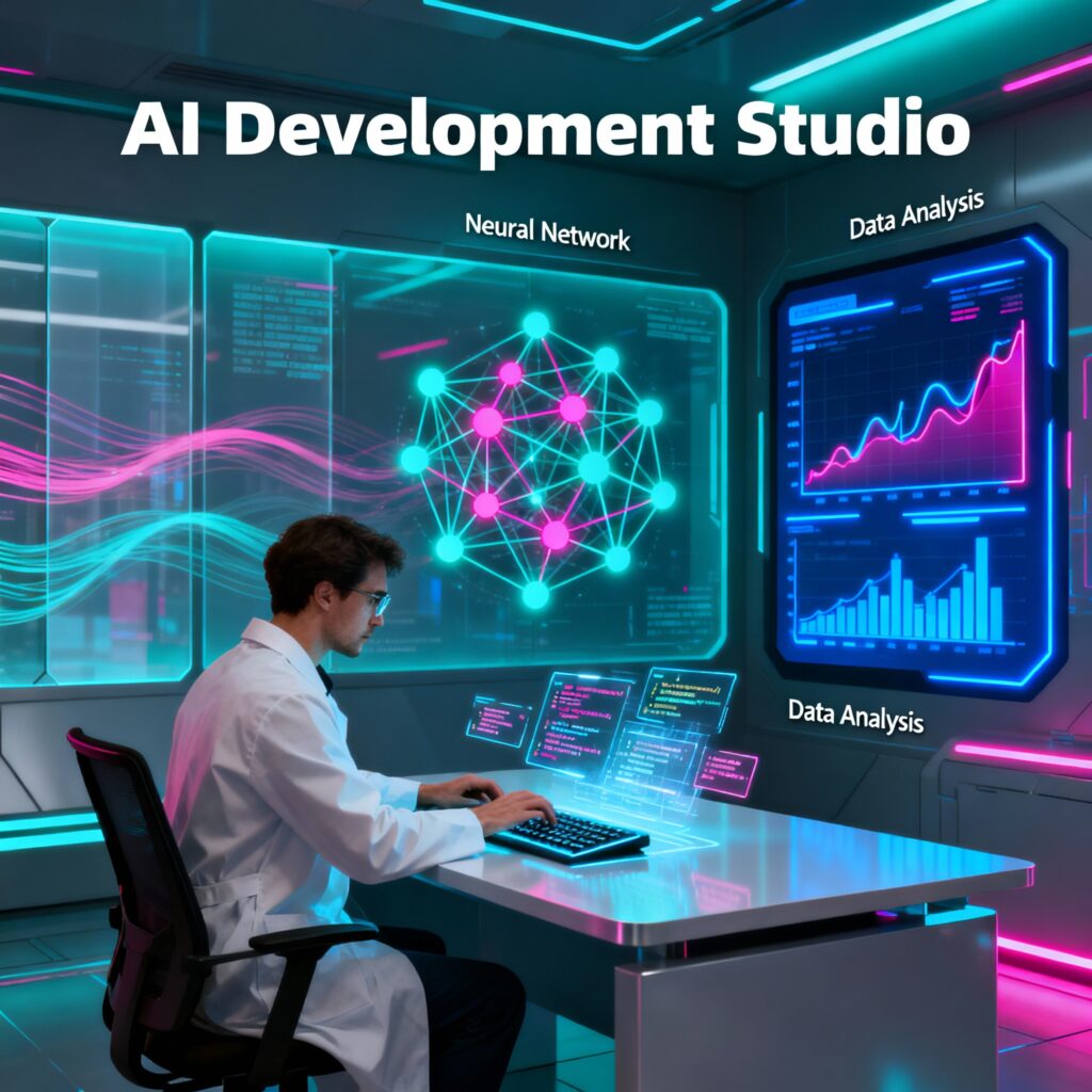
As the industry embraces digital transformation, HTL is also investing strongly in artificial intelligence and advanced software solutions to complement our hardware leadership. We are developing and deploying AI-driven technologies such as Automatic Defect Classification and Predictive Maintenance, integrating them seamlessly with our equipment platforms to deliver smarter, more reliable, and future-ready manufacturing environments. Alongside this, HTL India serves as a trusted partner for end-to-end software development—from concept to deployment—in industrial automation, semiconductor equipment software, enterprise applications, image processing, and AI-based systems. Our innovation is further strengthened by our patented AI-based solution for automatic photomask defect detection and classification, reflecting our commitment to digital excellence.
On behalf of the entire HTL India team, I extend my sincere appreciation to our customers, partners, and employees for their continued trust and collaboration. Together with the global HTL Group, we remain dedicated to delivering the most advanced technologies, best-in-class service, and fully integrated solutions that create measurable value—driving success for our customers and shaping the future of the semiconductor industry.
About HTL India
HTL Co. India Pvt. Ltd. was established in 2012 as a wholly owned subsidiary of HTL Co. Japan Ltd.
Building on the technological expertise and values of HTL Japan, HTL India plays a key role in supporting the Group’s global operations and growing customer base.
With a strong focus on technology and innovation, HTL India works closely with customers and partners to deliver reliable solutions and contribute to the sustainable growth of the HTL Group.
Our offices are located in:
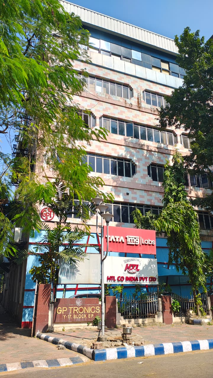
Bangalore – Head Office
Kolkata – Branch Office
Semiconductor Equipment Trading
Software Development
System Integration
With a deep understanding of the Japanese market and a growing presence in India and other global regions, we provide cutting-edge technology solutions that foster international collaboration in semiconductor innovation.
At HTL, we excel in understanding customer needs and connecting them with the right partners and technology providers. Our solutions combine innovation, precision, and reliability — ensuring that every engagement creates measurable value.
Tailored software solutions for semiconductor equipment System integration and automation services Hardware sales and after-sales support Collaborative R&D for advanced manufacturing systems
Since the establishment of our software development centers in Bangalore and Kolkata, we have been consistently delivering high-quality software, hardware sales, and support services to our customers worldwide. We are committed to: Meeting customer expectations on time and within budget Delivering cost-effective, high-quality solutions using leading-edge technologies Continuously improving our processes for sustained excellence Achieving customer satisfaction through innovation and quality assurance
At HTL, we believe that our success lies in the success of our customers and partners. By building strong relationships, sourcing the best talent, and investing in future-ready technologies, we continue to grow together — shaping the future of semiconductor innovation.

HTL Japan was founded by President Acharya to provide high-technology trading and liaison services in the semiconductor industry.
Software Development Center
Started Business of Plasma related Equipments of PVA TePla AG.(old name Asyntis)
Started Business of Atomic Layer Deposition (ALD) Equipment of Arradiance Inc.
Bangalore Head Office
Kolkata Branch Office
Started Business of Photomask Repair Machine of V-Technology
Started Business of Laser 3D Printer of RPM Innovations, Inc.
Established a local subsidiary in USA
Established a local subsidiary in China
Established a local subsidiary in Sweden
Clean room class 1000-10000
Established a local subsidiary in the Korea
Established a local subsidiary in Taiwan
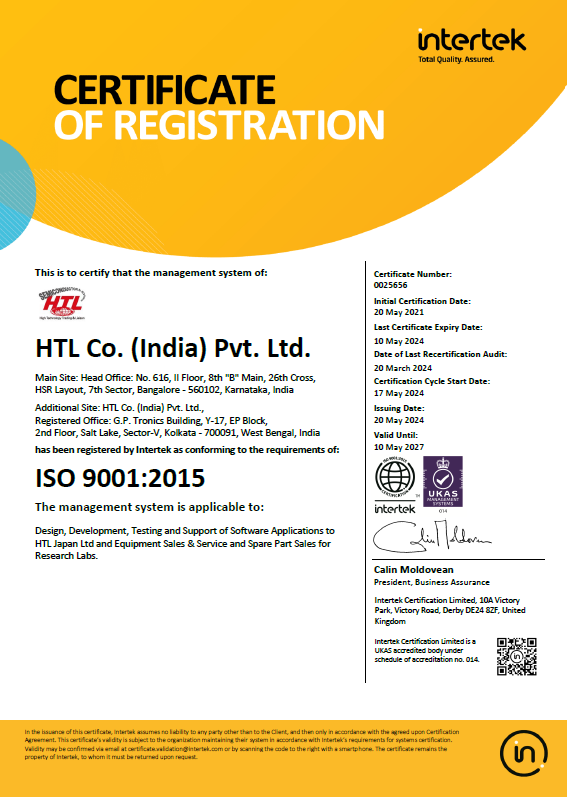
HTL Co. India operates under a structured Quality Management System (QMS) and is certified to ISO 9001:2015 standards by Intertek, accredited by UKAS.
This certification reflects our commitment to delivering consistent quality, ensuring customer satisfaction, and continuously improving our processes across semiconductor equipment solutions, software engineering services, and system integration.
ISO 9001:2015 Certified
Intertek Certified | UKAS Accredited
HTL Co. India is a proud member of SEMI (Semiconductor Equipment and Materials International), the global industry association representing companies across the semiconductor manufacturing supply chain.
Through our membership, we stay connected with industry standards, global technology trends, and collaborative initiatives that drive semiconductor innovation.
Photomask, Semiconductor equipment, FPD, OSAT, ALD system and 3D printers.
Software development for inspection, repair, and lithography equipment — primarily for Japanese clients.

Specialized semiconductor domain training for college graduates — focusing on photomask and lithography technologies.
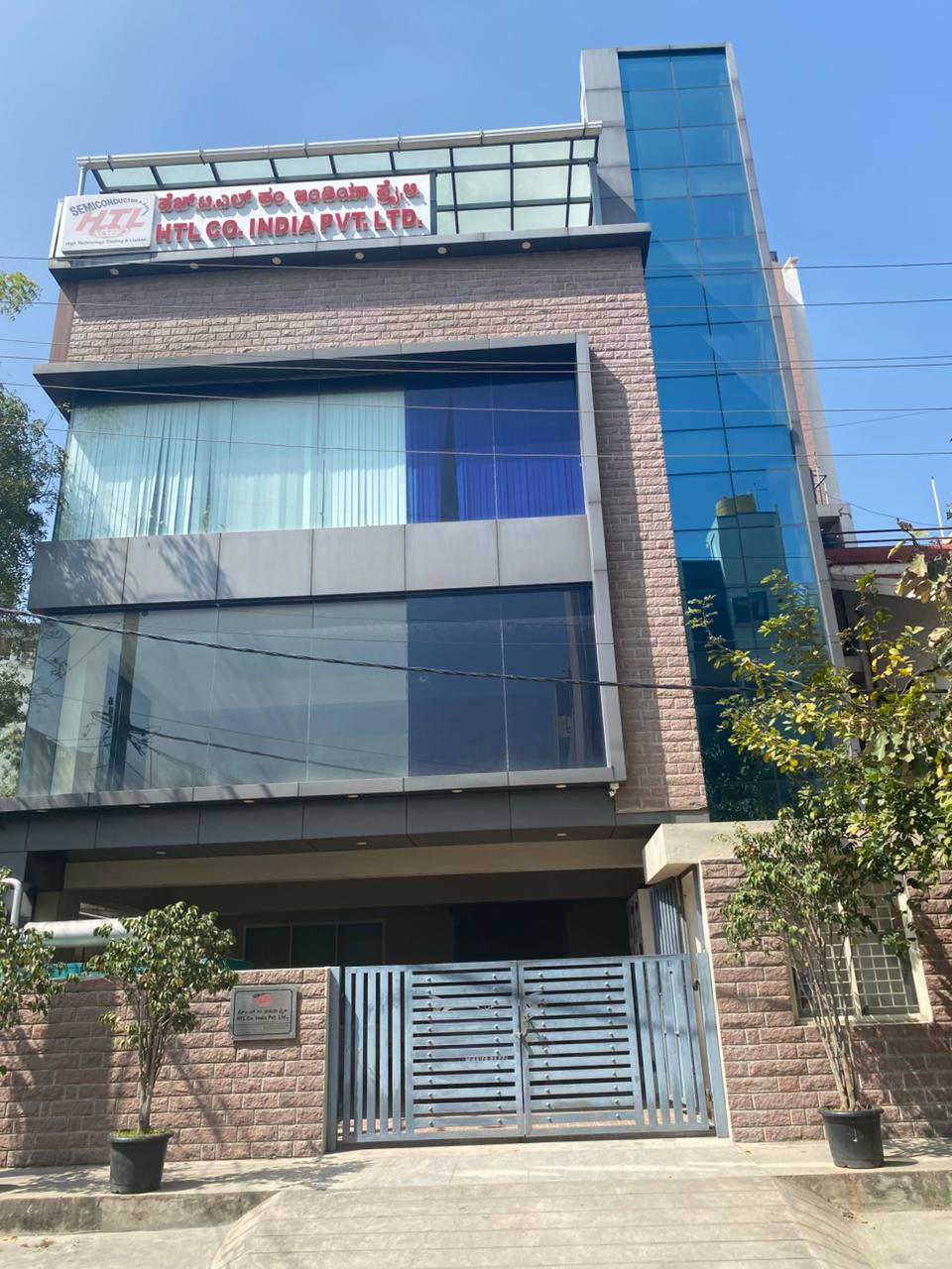
Own building with software and hardware divisions, including a semiconductor cleanroom with a photolithography mask writer.
Dedicated offshore development center supporting Japanese clients with software projects.
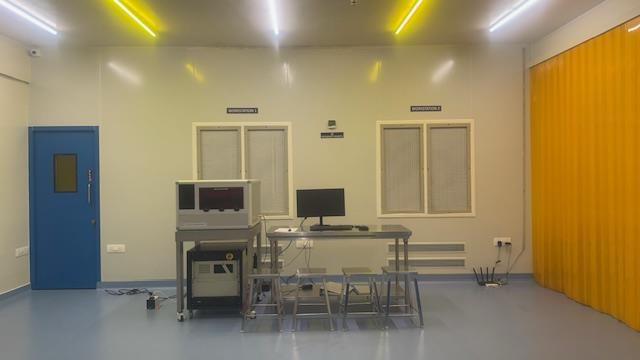
Our Bangalore facility houses a dedicated cleanroom lab equipped with advanced semiconductor tools.
To be a trusted global partner in semiconductor technology and innovation.
HTL is committed to deliver cost effective, innovative solutions of high quality consistently ensuring highest customer satisfaction while enabling us to be among the best of global technology solution companies.
Customer focus, quality commitment, cultural respect, and continuous improvement.
HTL has a strong international footprint — with presence in Japan, India, China, Korea, Taiwan,
Sweden, and the USA.


ISO 9001:2015 Certified Quality Management System
Certified by Intertek – UKAS Accredited
© 2026 HTL Co India Pvt. Ltd. All Rights Reserved.