
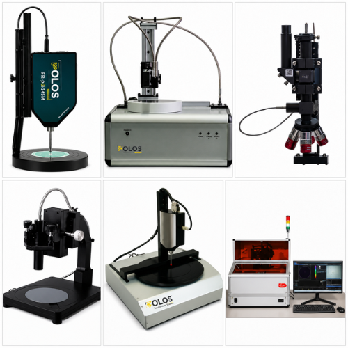
The SPS POLOS Film Characterization Series provides high-precision, non-contact measurement solutions for thin-film thickness analysis, optical characterization, and wafer mapping applications. Designed for semiconductor, MEMS, photonics, nanotechnology, and advanced materials research, these systems deliver fast, accurate, and repeatable measurements for process development and quality control.
Available in portable, table top, and automated wafer mapping configurations, the platform supports single-point thickness measurement, reflectance, transmittance, absorbance analysis, and full wafer characterization across a wide range of thin-film materials.
Accurate characterization of thin films, coatings, multilayer structures, and functional materials with non-contact optical measurement technology.
Benefits
Choose from compact single-point measurement systems or advanced wafer mapping platforms for comprehensive substrate characterization.
Depending on the model, measurement ranges extend from 190 nm to 1700 nm, enabling analysis of diverse materials and coating structures.
Portable and table top systems provide flexible deployment in laboratories, cleanrooms, production facilities, and research environments.
Supports a wide range of measurement configurations for evolving research, process development, and manufacturing requirements
Characterization of photoresists, dielectric layers, thin films, and multilayer structures for process development and quality assurance.
Ideal for nanomaterials, functional coatings, optical films, and emerging material technologies.
Measurement of optical coatings, waveguide structures, transparent films, and photonic devices.
Widely used in universities, R&D centres, cleanrooms, and industrial laboratories for material characterization and process optimization.
Model | Thickness Range | Spectral Range | System Type |
FR-pOrtable | 12 nm – 90 μm | 380 – 1020 nm | Portable |
FR-pRo | 1 nm – 120 μm | 190 – 1100 nm | table top |
FR-Mic | Customized Configuration | Customized Configuration | Microscope-Based System |
FR-ES | 12 nm – 500 μm | 370 – 1700 nm | table top |
FR-Scanner | 3 nm – 100 μm | 200 – 1020 nm | Table top |
FR-SCANNER-AIO-MIC-XY200 | 4 nm – 150 μm | 200 – 1700 nm | Automated Table top |


ISO 9001:2015 Certified Quality Management System
Certified by Intertek – UKAS Accredited
© 2026 HTL Co India Pvt. Ltd. All Rights Reserved.