
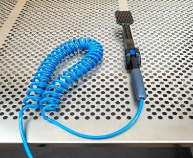
The SPS POLOS Vacuum Wand Series provides safe, contamination-free handling of wafers, photomasks, dies, and delicate substrates used in semiconductor manufacturing, MEMS fabrication, photonics, and research laboratories.
Designed with ESD-safe materials, ergonomic handling, and cleanroom compatibility, these vacuum wand sets enable precise substrate transfer while minimizing particle contamination, handling damage, and operator errors. Compatible with standard facility vacuum supplies, the systems are ideal for both R&D and production environments.
Vacuum-assisted pickup and placement minimizes direct contact with sensitive substrates, reducing the risk of scratches, particles, and wafer damage.
Manufactured using antistatic materials for safe handling of semiconductor wafers and electronic devices.
Benefits
Available configurations support applications ranging from micro-devices and dies to full 300 mm semiconductor wafers.
Specialized configurations are available for compound semiconductors, thin wafers, and delicate substrates requiring low-stress handling.
Lightweight construction and precision grip designs improve operator comfort and handling accuracy during repetitive tasks.
Safe transfer of wafers during inspection, lithography, metrology, packaging, and process tool loading.
Precise handling of sensitive substrates used in MEMS, sensors, and advanced microfabrication workflows.
Ideal for semiconductor dies, optical components, micro-packages, and small device handling.
Suitable for ISO Class 3 and ISO Class 4 environments in universities, R&D facilities, and semiconductor fabs.
Product Number | Supported Size | Type | Configuration | ISO Class |
WHS-V2-SET-SD | Small Devices & Dies | Set | Precision Handling | ISO 4 |
WHS-V2-SET100C | 76–100 mm Wafers | Kit | Straight Grip | ISO 3 |
WHS-V2-SET200 | 150–200 mm Wafers | Set | Straight Bend | ISO 3 |
WHS-V2-SET200C | 150–200 mm Thin/Compound Wafers | Set | Straight Bend | ISO 3 |
WHS-V2-SET300 | 300 mm Wafers | Set | Straight Bend | ISO 3 |


ISO 9001:2015 Certified Quality Management System
Certified by Intertek – UKAS Accredited
© 2026 HTL Co India Pvt. Ltd. All Rights Reserved.