HTL India bridges the gap between academia and the semiconductor industry through specialized, hands-on training programs in Photomask Technology, Lithography, and Equipment Software Integration — designed for college graduates and young professionals.
Our Training & Education Division has been established to prepare future engineers with the practical knowledge, process awareness, and technical confidence required to work on cutting-edge semiconductor manufacturing equipment.
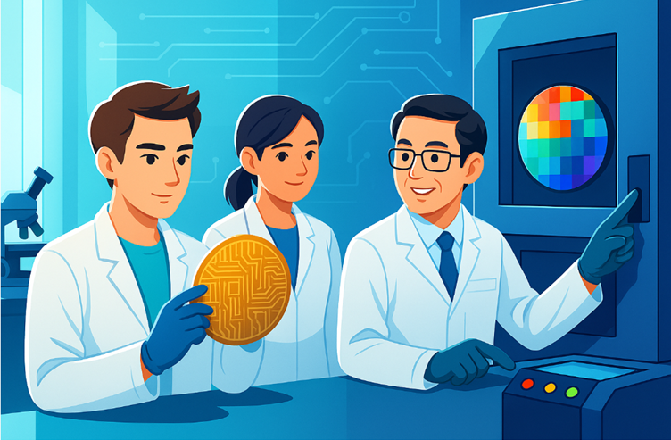
HTL India’s programs are built upon our decades of experience in photomask inspection, repair, and writing systems, developed in close collaboration with our Japanese headquarters (HTL Japan) and global semiconductor equipment partners.

Build foundational knowledge of semiconductor manufacturing and mask fabrication.
Offer hands-on exposure to photomask equipment and lithography systems.
Teach software concepts relevant to semiconductor equipment (control, image processing, AI).
Develop industry-ready engineers who can join semiconductor R&D or equipment companies immediately after graduation.
Bridge theory with practice using real industrial examples and case studies.
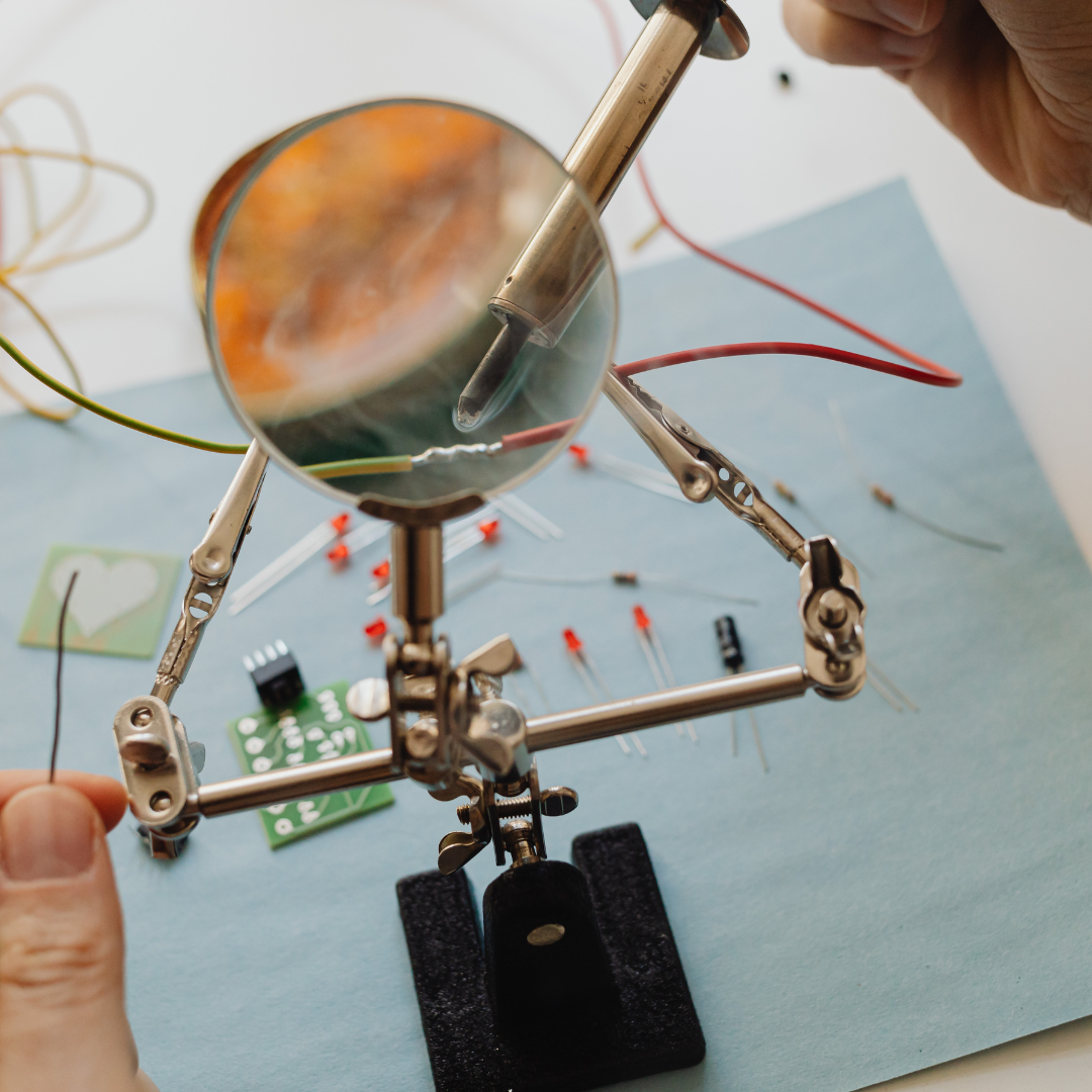
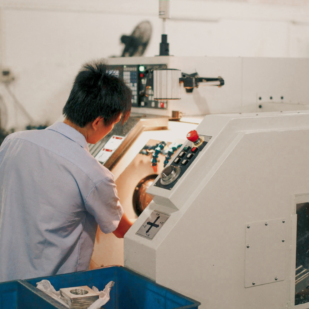
Students are trained using simulation tools, live demonstrations, and equipment models installed in HTL India’s cleanroom setup.
This includes exposure to:
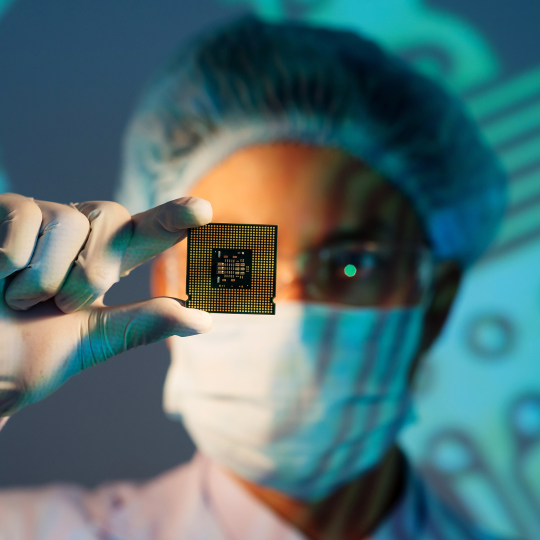
This program introduces students to mask materials, pattern generation, defect types, and the end-to-end mask manufacturing flow. Participants gain industry-relevant knowledge on critical processes such as pattern writing, etching, cleaning, and inspection using real-world examples from semiconductor R&D environments. Ideal for students aspiring to work in mask shops, lithography labs, and semiconductor equipment companies.
Joint certification and placement linkages are available for partner institutions.
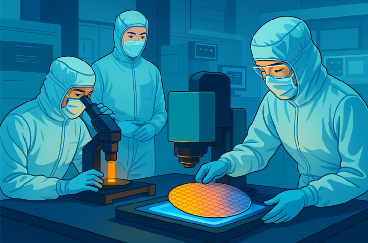
Gain a strong foundation in the core processes that drive modern semiconductor fabrication. This module covers photoresist chemistry, exposure systems, alignment techniques, pattern transfer, etching fundamentals, and cleanroom practices. Students learn how lithography shapes every device layer and understand the critical process parameters that affect yield and device performance. Ideal for graduates aiming to work in fab operations, lithography labs, or semiconductor equipment roles.
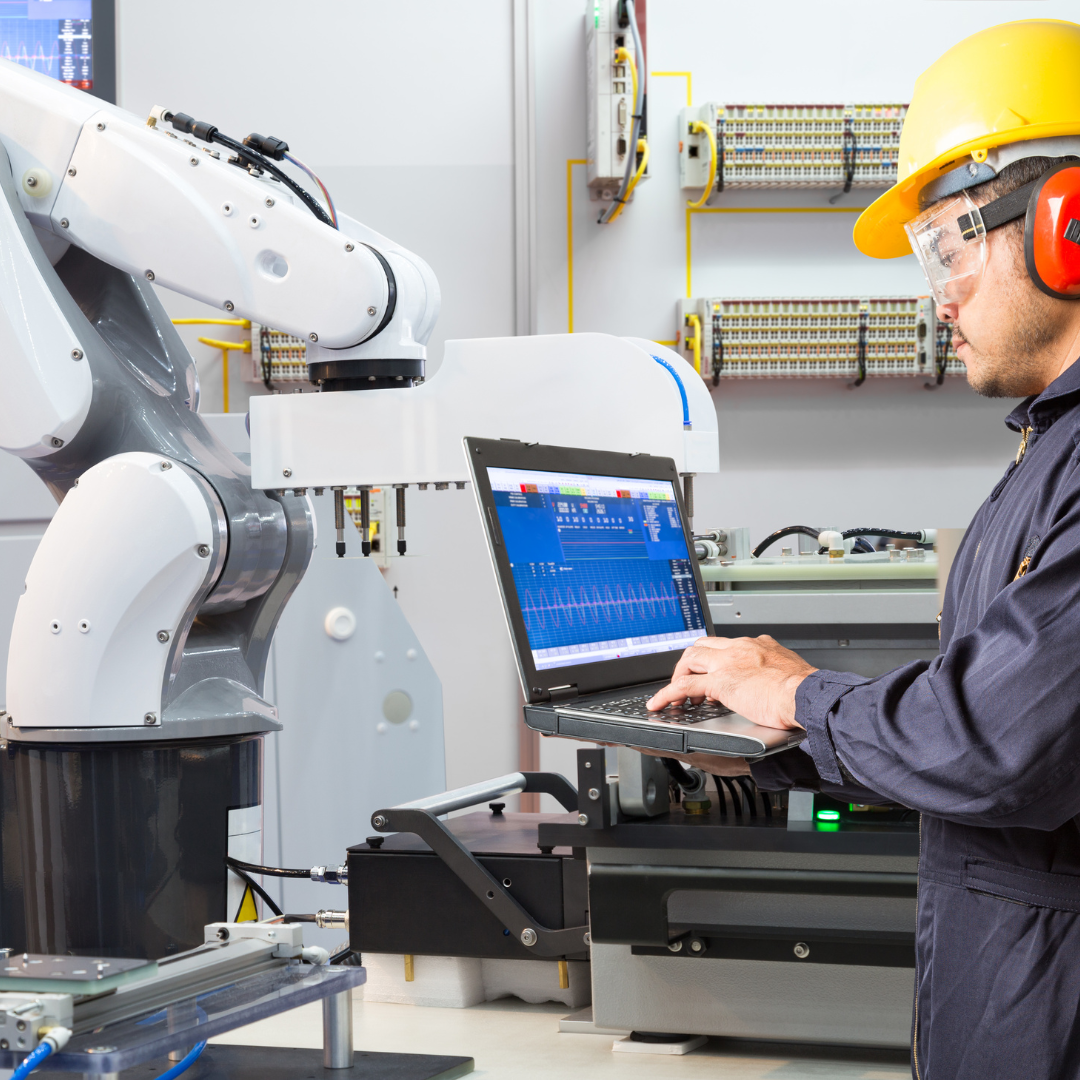
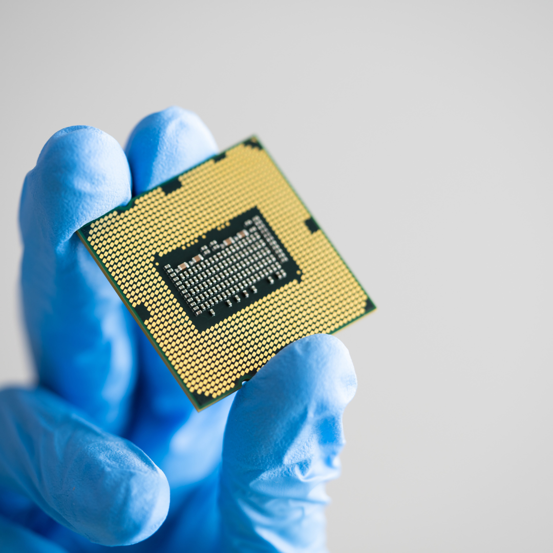
Learn how semiconductor manufacturing equipment and control software work together to create precise, repeatable processes. This module introduces students to embedded control concepts, machine interfaces, motion systems, sensors, and real-time data handling. Trainees gain hands-on understanding of how inspection, lithography, and mask-writing machines integrate hardware with firmware, drivers, and application software — preparing them for real-world equipment engineering roles.

HTL India is actively in the process of collaborating with:
Upon completion, trainees can pursue roles such as:
HTL India’s HR and Operations teams provide:


ISO 9001:2015 Certified Quality Management System
Certified by Intertek – UKAS Accredited
© 2026 HTL Co India Pvt. Ltd. All Rights Reserved.