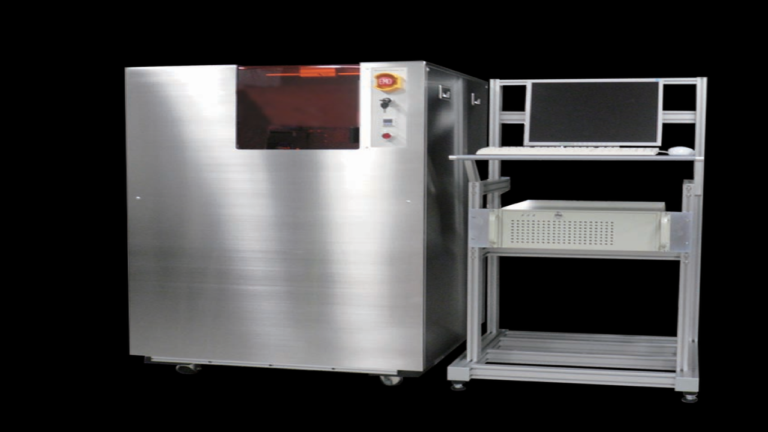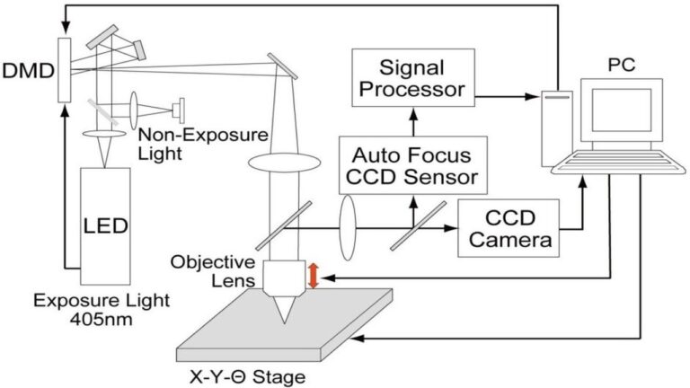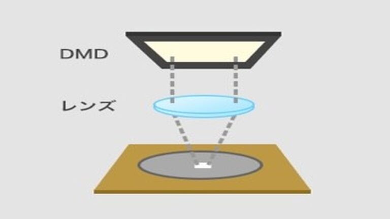
Nanosystem Solutions, Inc. Japan was established in December of 2004 with support from the National Institute of Advanced Industrial Science and Technology. With a focus on our unique optical technology at our core, we started as a research and development venture that addresses needs using specialized technology in the fields of nano manufacturing and measurement. Presently, we operate in the business of maskless lithography equipment, which is lithography equipment utilizing digital micro mirror devices (DMD) and not requiring masks.
Features:
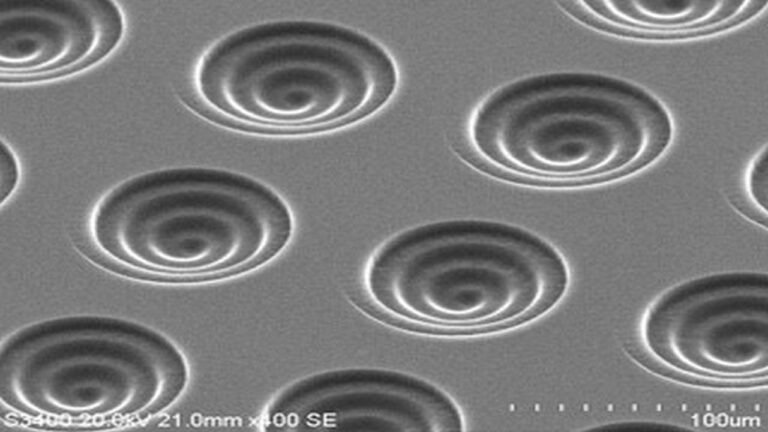
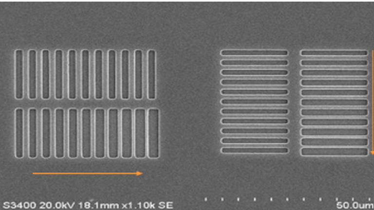
- 1um resolution(0.5um or 2um resolution are the option)
- Both Scanning and Step & Repeat mode are available
- Maintenance Free System by the use of Long Life Light Source (LED or semiconductor Laser)
- High Speed patterning speed > 2000mm 2/min (Laser Light Source)
- Our smart real-time Auto Focus able to pattern even on the thin-transparent substrate, patterned substrate, and warped substrate
- Simultaneous observation of surface pattern and exposure pattern by coaxial observation system, TTL(Through The Lens) and it allows high accuracy overlay with our own image processing technology.
- Data convertor for DXF and GDSII is available.
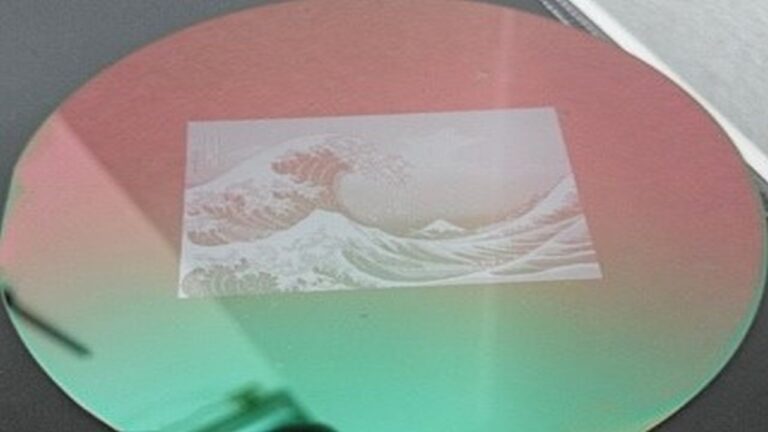
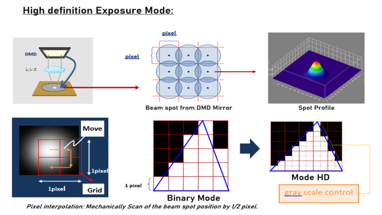
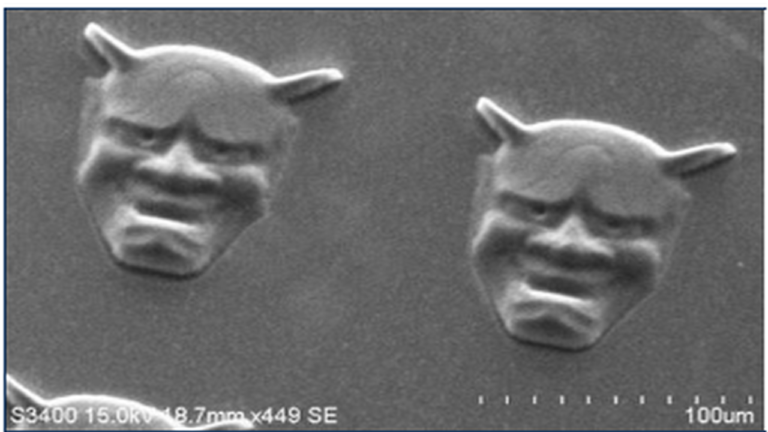
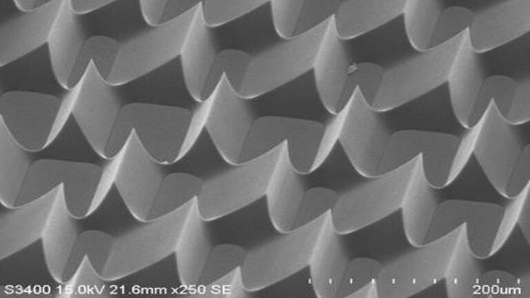
- Gray Scale Image can be exposed for 3D structuring
- Down to 12.5nm address grid unit
- Wide range of substrate Size: few mm up to metric size
Applications:
- Photo semiconductor device development
- Development of communications devices
- Development of light-curing materials
- Micro ID numbering
- MEMS
- Bio, Life science, complex chemistry (Micro TAS, Microfluidics)
- Localized exposure and selective exposure applications, etc.
- Mix & Match with Ebeam Lithography
- Industrial field
(reticle and photomask production, micro mold, compound semiconductor fabrication, etc.)
For more details please visit the parent website: https://www.nanosystem-solutions.com
For enquiries, please send us an email to sales@htlco.co.in